|

 The oscillation circuit
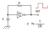
The inverter which has the hysteresis characteristic is
used as the oscillation circuit. The output wave form of the oscillator
is the square wave. The oscillation frequency can be changed by VR1. The
control of the oscillation frequency is used for the adjustment of the
output voltage. The circuit which was made this time could be changed
from 334KHz to 12,650KHz. The frequency with the upper limit depends on
the high frequency characteristic of the IC.
As for the operation of the oscillator which used the
inverter, refer to "Square wave oscillator".
The current amplification circuit
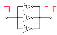
It depends on the kind of the IC but the many electric
currents which are gotten from the one inverter don't occur.
In case of 74HC14, the maximum electric current which can
be passed with the inverter of the 1 circuit is 4 mA. Because it is, the
one inverter is OK but connects the inverter in parallel for the safety.
In case of 74HC14, the six inverters are housed in the one package. At
the circuit this time, the four inverters are connected in parallel. The
inverter immediately behind the inverter for the oscillation is for the
buffer. It is the one to make that the change of the load current
influences the oscillation little. I think that it is permitted to do
the five inverters in the multiple connection without using the buffer.
Generally, among the output of the logic circuit aren't
connected. It is because the output competes when the different signal
is inputted and the IC has broken.
In case of the circuit this time, because all input
signals are the same, they can connect the output in parallel. However,
strictly, it is not the good way.
The resonance circuit
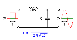
As for the square wave signal which was made with the
oscillator, the maximum voltage is 5Vp-p(Low:0V, High:+5V). current
signal by the resonance circuit which used the coil and the capacitor.
The positive and the negatively changing alternating
current signal are composed of the resonance circuit. The resonant
frequency becomes the frequency to take out.
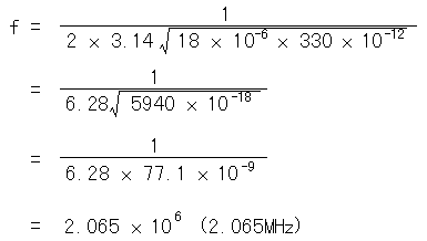
The resonant frequency is calculated in
 . When
calculating as L = 18 µH, C = 330 pF, the resonant frequency becomes
about 2 MHz. . When
calculating as L = 18 µH, C = 330 pF, the resonant frequency becomes
about 2 MHz.
At the circuit which I made, the resonant frequency was
2,140 KHz.
The voltage amplification rectification circuit
This is the circuit which gets about twice of DC voltages
from the inputted alternating voltage.
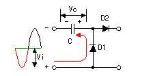
In the period with the negative voltage of the input
alternating current signal, the electric charge is stored up to the
capacitor (C) through D1. With this, the voltage of the both edges of
the capacitor becomes Vc.
Next, in the period with the positive voltage with the
input alternating voltage, the input voltage (Vi) and the voltage (Vc)
of the capacitor are gained and the voltage of Vi+Vc is output.
The value of Vi and Vc are changed by the frequency of
the input alternating current or the electric current which flows
through the load.
The circuit this time works in the high frequency
switching. Because it is, as the diode, the shottky barrier diode with
the short recovery time must be used.
The ripple filter circuit
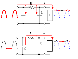
As for the DC voltage which is output from the voltage
amplification rectification circuit, the half wave was rectified. So,
the ripple is contained in the output. The ripple filter circuit is used
to make this ripple little. The circuit this time is using the resistor
instead of the coil. Therefore, the output voltage falls at more when
the output current increases.
|